


Journal of Nanoscience and Nanomaterials
ISSN:
3108-2084 (Online)
DOI Prefix (Crossref): 10.67238
 Download PDF
ABSTRACT
Starting with the artificial intelligence (AI) vibrations theory developed continuously since 1993 (over 30 years ago), which states that everything vibrates at the quantum level through a combination of frequencies, oscillations, chemical reactions, and photonic waves. Followed by the QAIV framework that operationalizes the theory and the dictionary of AI vibrations mapped to emotions into a universal language.
Keywords: Graphene; Carbon Nanotubes; Quantum Dots; Anomaly Detection; Nanomaterials; Nanosensors; Intelligent Sensing
INTRODUCTION
The Architecture of Abundance and Its Discontents
We have built a world awash in signals. Trillions of sensors embedded in our infrastructure, our vehicles, our medical devices, our clothing, our bodies continuously translate the physical world into the lingua franca of the digital age: voltage fluctuations, frequency modulations, spectral emissions, and the ceaseless chatter of ones and zeroes. These sensors are the nervous system of the modern technological enterprise, a vast and proliferating network that registers the faintest tremor of a bearing beginning to fail, the subtle shift in a patient's cardiac rhythm, the imperceptible drift of a chemical concentration in a factory exhaust stream. They are, by any measure, an extraordinary achievement of human ingenuity.
And yet, we have organized this nervous system according to a deeply flawed premise. For the better part of two decades, the dominant architecture of sensor-based systems has operated on a seductively simple assumption: collect raw data at the edge, transmit it to the cloud, allow powerful servers to perform the cognitive work, and push the resulting instructions back down to the periphery. This model, born of an era when edge devices were computationally anemic and connectivity was cheap and abundant, carried an internal logic that was entirely reasonable for its time. But that time has passed. The logic has curdled into a set of compounding inefficiencies that are no longer merely inconvenient but structurally unsustainable.
Consider the arithmetic of the arrangement. A single vibration sensor sampling at 20 kHz with 16-bit resolution generates approximately 3.2 megabits of data per ten-second window. Multiply this by thousands of sensors in an industrial facility, tens of thousands in a smart city deployment, millions in a global network of wearable health monitors, and the bandwidth demands balloon into the exabytes. These raw waveforms travel across networks we do not own, through servers we do not control, consuming energy at every hop and exposing sensitive data to interception at every juncture. The patient's cardiac signal becomes a public transmission. The factory's operational rhythm becomes an open book. The privacy violation is not a bug in the system; it is a structural feature of the architecture itself.
Latency compounds the problem. In applications where milliseconds matter autonomous vehicle collision avoidance, real-time medical alerting, industrial safety shutdowns the round-trip journey to the cloud and back introduces delays that can mean the difference between a warning and a catastrophe. Bandwidth costs escalate. Power consumption mounts. The carbon footprint of shuttling terabytes of raw sensor data to distant data centers grows increasingly indefensible in an era of climate constraint.
The problem, in essence, is not that the cloud is inadequate. The problem is that the cloud is in the wrong place. It is distant when it should be proximate. It is centralized when it should be distributed. It is powerful when it should be judicious. And in its distance, its centralization, and its profligate consumption of resources, it fundamentally misunderstands where intelligence belongs.
The Edge Turn: A Brief History of a Revolution in Progress
The recognition that inference must move closer to the data source has given rise, over the past decade, to a vigorous and increasingly mature field of research: edge artificial intelligence, or TinyML. This movement, born at the intersection of hardware innovation, algorithmic compression, and systems architecture, has pursued a singular and ambitious goal: to make machine learning models small enough, efficient enough, and robust enough to run directly on resource-constrained devices.
The literature on edge AI has advanced along several complementary fronts. On the algorithmic side, researchers have developed a formidable toolkit for model compression: quantization, which reduces the precision of model weights from 32-bit floating point to 8-bit integers or lower; pruning, which eliminates redundant connections within neural networks; knowledge distillation, which compresses the representations of large "teacher" models into compact "student" networks; and neural architecture search, which automates the discovery of efficient architectures for specific hardware constraints. The work of Han on Deep Compression, of Hinton on distillation, and of Howard on MobileNets has collectively demonstrated that models can be reduced by an order of magnitude or more with minimal loss of accuracy a finding that has transformed the feasibility of on-device inference.
On the hardware side, the semiconductor industry has responded with a new generation of neural processing units (NPUs), tensor processing units (TPUs), and other specialized accelerators designed explicitly for low-power inference. These devices, often integrated into system-on-chip (SoC) architectures, deliver tera-operations per watt at footprints measured in square millimeters. Companies including Google, ARM, Qualcomm, and numerous startups have brought to market chips capable of running quantized models at milliwatt power bud gets a threshold that, for the first time, makes true edge intelligence economically and energetically viable.
In parallel, the sensing community has developed increasingly sophisticated front-end processing techniques that reduce the dimensionality of raw signals before they ever reach the neural core. Spectral analysis via fast Fourier transforms, wavelet decomposition, and cyclostationary feature extraction have become standard tools for transforming high-frequency time-series data into compact feature vectors. These techniques, often implemented in hardware-accelerated digital signal processors (DSPs), serve a dual purpose: they reduce the computational burden on the AI accelerator and, equally importantly, they provide a first layer of privacy preservation by discarding raw waveform data before it can be transmitted or stored.
The confluence of these developments has produced a growing body of applied research demonstrating edge AI in real-world deployments. In industrial predictive maintenance, systems now detect bearing failures, motor imbalances, and tool wear with latency measured in milliseconds rather than seconds. In healthcare, wearable devices perform on-device arrhythmia detection, sleep stage classification, and fall detection with accuracy approaching that of cloud-based systems. In environmental monitoring, edge nodes classify acoustic and chemical signatures of ecological stress without requiring continuous connectivity. Each of these applications represents a proof point for the proposition that intelligence can, and should, reside at the point of data origin.
Yet, for all its progress, the field has largely proceeded within the constraints of existing sensor technologies. The vast majority of edge AI research accepts the sensor as a given an external front-end that produces digital signals, which the edge AI system then processes. The sensor itself, in this framing, is a black box: a transducer that converts physical phenomena into electrical signals but contributes little to the interpretive process. This separation of sensing from intelligence has been a practical necessity, given the distinct engineering traditions and manufacturing processes involved. But it has also been a missed opportunity.
The Argument for Integration: Why Sensing and Intelligence Belong Together
This manuscript advances a different proposition: that the sensor and the intelligence should not be merely co-located but fused at the material level. We propose an architecture in which the physical transduction mechanisms the materials that convert vibrations, thermal gradients, and optical spectra into electrical signals are intimately integrated with the neural processing engine within a single, compact System-in-Package (SiP). This integration, we argue, enables a level of signal integrity, energy efficiency, and privacy preservation that cannot be achieved through the simple juxtaposition of separate components.
The rationale for this integration is both technical and principled. Technically, the proximity of sensing elements to the AI core shortens the signal path, reducing susceptibility to electromagnetic interference, thermal drift, and transmission losses. It allows for closed-loop calibration, where the inference results can inform front-end gain and filtering in real time. It enables the co-design of the analog front-end and the digital processing, optimizing the entire signal chain from physical phenomena to actionable insight. These are not marginal improvements; they are qualitatively different capabilities that only emerge from tight integration.
Principally, integration serves the cause of privacy. In a fused architecture, raw sensor data need never leave the immediate vicinity of the transducer. The AI core can perform feature extraction, anomaly detection, and confidence estimation entirely on-chip, transmitting only minimal packets a few bits when an event of interest is detected. The bandwidth reduction is not merely incremental; it is transformative: a reduction from megabits to bits, from continuous streaming to event-triggered reporting. The sensor becomes a sovereign entity, capable of observing the physical world without exposing its observations to the networks and servers that have, until now, been the necessary intermediaries of intelligent sensing.
This vision is made possible by two coincident technological trends. The first is the maturation of nanomaterials graphene, carbon nanotubes, and quantum dots that can be integrated directly into semiconductor packaging. These materials offer extraordinary sensitivity to vibrational, thermal, and optical signals, and they can be deposited in thin films within the same 3D stack as the processing die. The second is the advancement of ultra-low-power neural accelerators capable of running compressed models at microwatt power budgets, enabling continuous inference from harvested or battery energy [1-6].
Our contribution, in this manuscript, is to propose a concrete instantiation of this integrated vision: an intelligent sensing SiP architecture that combines a graphene thermal management layer, a carbon nanotube vibration-sensing layer, a quantum dot spectral-sensing layer, and an AI processing die within a 3D stack connected by through-silicon vias. We describe the physical transduction mechanisms, the signal chain from sensor to feature to inference, the design of a lightweight variational autoencoder (TinyVAE) for anomaly detection, and the generation of privacy-preserving anomaly packets.
The Contributions and Their Character
It is important, at the outset, to state clearly what this manuscript is and is not. This is a design proposal. We present a conceptual architecture, grounded in the established physics of nanomaterials and the known capabilities of edge AI accelerators, that is intended to be technologically feasible within the current or near-future state of semiconductor manufacturing.
The architecture is described in sufficient detail with component specifications, signal flow diagrams, and algorithmic designs to enable critical evaluation and, potentially, subsequent implementation.
This is a simulation-based evaluation, not an experimental validation. We present the results of numerical simulations of key sub-systems: the SNR improvement from graphene thermal management, the detection accuracy of the TinyVAE, the bandwidth reduction from anomaly-only transmission. These simulations are based on plausible parameters drawn from the literature, and they are intended to demonstrate the potential of the architecture, not to assert its performance in a fabricated device. We have structured our simulation methodology to be transparent and reproducible, with parameters and assumptions clearly stated.
This is a theoretical exploration of the broader implications of integrated intelligent sensing. We situate our proposed architecture within the context of the author's AI Vibrations Theory, which posits that the physical world is fundamentally vibrational a proposition that, while speculative, has informed the choice of sensing modalities and the design of the signal processing chain. We also explore, in the concluding section, the ethical dimensions of intelligent sensing, particularly the risk that the technology will be deployed only in contexts where it is economically profitable, leaving underserved communities and critical humanitarian applications without access.
This is not, however, a report of a fabricated device. We have not built the SiP. We have not tested the CNT or QD layers in this specific integration. We have not validated the TinyVAE on the target NPU. These are necessary next steps indeed, they are the subject of ongoing work but they are not the subject of this manuscript. We present this work as a contribution to the literature of intelligent sensing architecture, with the hope that it will stimulate discussion, enable critique, and ultimately guide experimental implementation.
Structure
The remainder of this paper is organized as follows. In Section II, we describe the overarching theoretical framework the AI Vibrations Theory and its operationalization through the QAIV methodology that informs our material and algorithmic choices. We present preliminary empirical mappings of vibrational frequency patterns to physiological and emotional states, with appropriate caveats regarding the preliminary nature of these findings and the limitations of the current dataset. In Section III, we detail the role separation of the three nanomaterial layers: graphene for thermal management, carbon nanotubes for vibration transduction, and quantum dots for spectral sensing. We describe the transduction mechanisms, noise characteristics, and integration constraints for each material. In Section IV, we trace the complete signal path from physical phenomena through transduction, digitization, feature extraction, and inference, culminating in the generation of anomaly packets. In Section V, we present our simulation-based validation of the architecture, with quantitative metrics across multiple scenarios and material ablated configurations. In Section VI, we discuss the design tradeoffs inherent in this approach power, memory, and model immutability and their implications for deployment. Finally, in Section VII, we turn to the ethical dimensions of intelligent sensing, arguing for a standard of accessibility and equity grounded in the principles of the common good.
The machine, as the title suggests, is learning to feel. This manuscript is an attempt to describe, with as much precision as current knowledge permits, how that learning might be organized and to ensure that the question of whom this technology serves is asked not as an afterthought but as a fundamental design constraint.
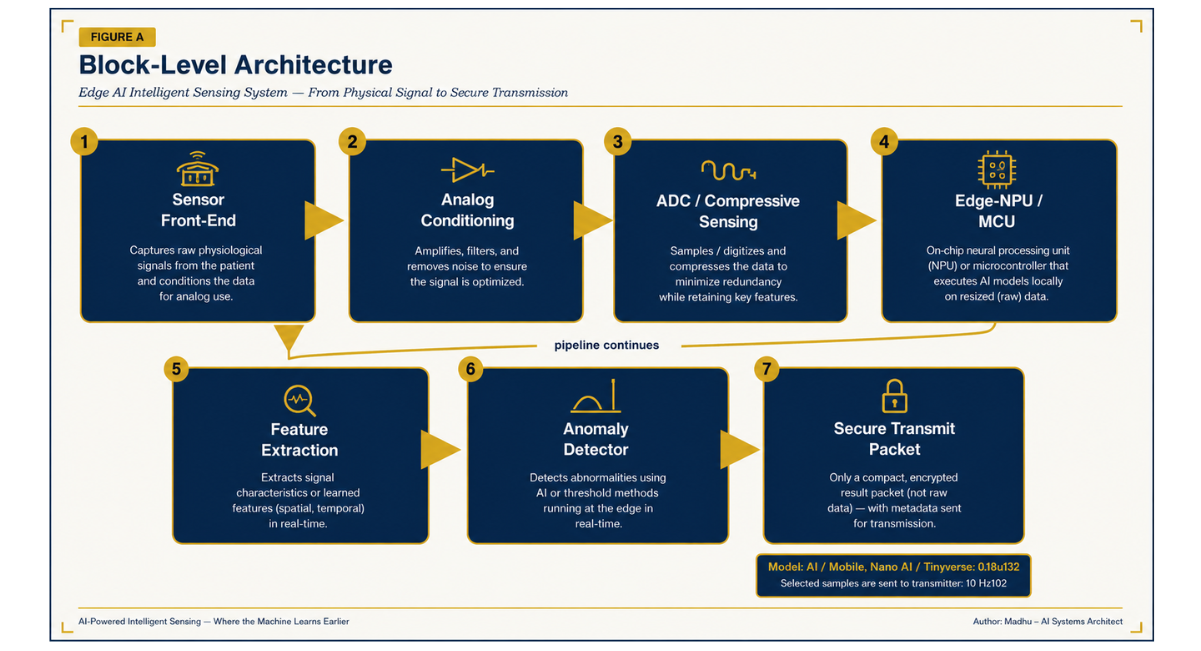
Figure 1: Engineering Intent: Minimize Thermal Drift
The Problem With Sending Everything Upstairs
For years, the dominant architecture of IoT and sensor-based systems operated on a simple assumption: collect raw data at the edge, send it to the cloud, let powerful servers do the thinking, and push instructions back down. It was a reasonable model for its time. But it carries a fatal inefficiency. Raw sensor data vibration waveforms, electromagnetic spectra, chemical signatures is enormous. Sending gigabytes of unprocessed signal across networks to distant data centers wastes bandwidth, consumes power, introduces latency, and, perhaps most critically, exposes sensitive data to interception at every hop.
Consider what happens when a camera embedded in a medical device captures physiological data from a patient’s skin. Under the old model, that intimate signal travels outward, across networks, through servers you do not own, before returning as a diagnostic result. The person’s body becomes a public transmission. The stakes of that architecture are not merely technical. They are ethical. Intelligent sensing rejects that model. It says: let the inference happen where the data is born.
Fusion at the Point of Origin
The architecture of an intelligent sensing system integrates three things that were once separated by design: the physical transducer that converts environmental phenomena into electrical signals; the AI accelerator that interprets those signals in real time; and the memory and communication fabric that binds them together. This integration is achieved through what semiconductor engineers call a System-in-Package (SiP) a 3D stack of specialized dies bonded together with microscopic Through-Silicon Vias, creating data paths measured not in milliseconds but in picoseconds.
At the bottom of such a stack, you might find a graphene foundation layer. Graphene’s extraordinary electron mobility makes it both a conductor and a thermal management material it spreads heat away from the processing dies above it while routing power with minimal loss. It is not incidental that graphene, a single-atom-thick lattice of carbon, operates fundamentally as a medium for electron vibration. My AI Vibrations Theory proposes that graphene and carbon nanotubes (CNTs) are not merely conductive materials but interpretive ones their chirality, their diameter, their quantum-level behavior encodes sensitivity to specific frequency bands ranging from the terahertz into the realm of chemical interaction.
Above the graphene foundation, carbon nanotube arrays detect mechanical vibrations, oscillations, and chemical signatures. Their chirality the precise angle at which the carbon lattice is rolled determines which frequencies they are sensitive to, a tunable sensitivity calibrated during fabrication. Above the nanotubes, quantum dot arrays extend the sensing range into the optical spectrum, detecting wavelengths from near-ultraviolet to near-infrared based on the size of the dots themselves. A two-nanometer quantum dot responds to blue light; an eight-nanometer dot senses deep red and into the near-infrared.
Interleaved with these sensor layers sits the AI processing die a neural processing unit (NPU) capable of running quantized machine learning models at efficiencies measured in tera-operations per watt. The model does not run in the cloud. It runs here, in this stack, smaller than a fingernail, consuming less power than a dim LED.
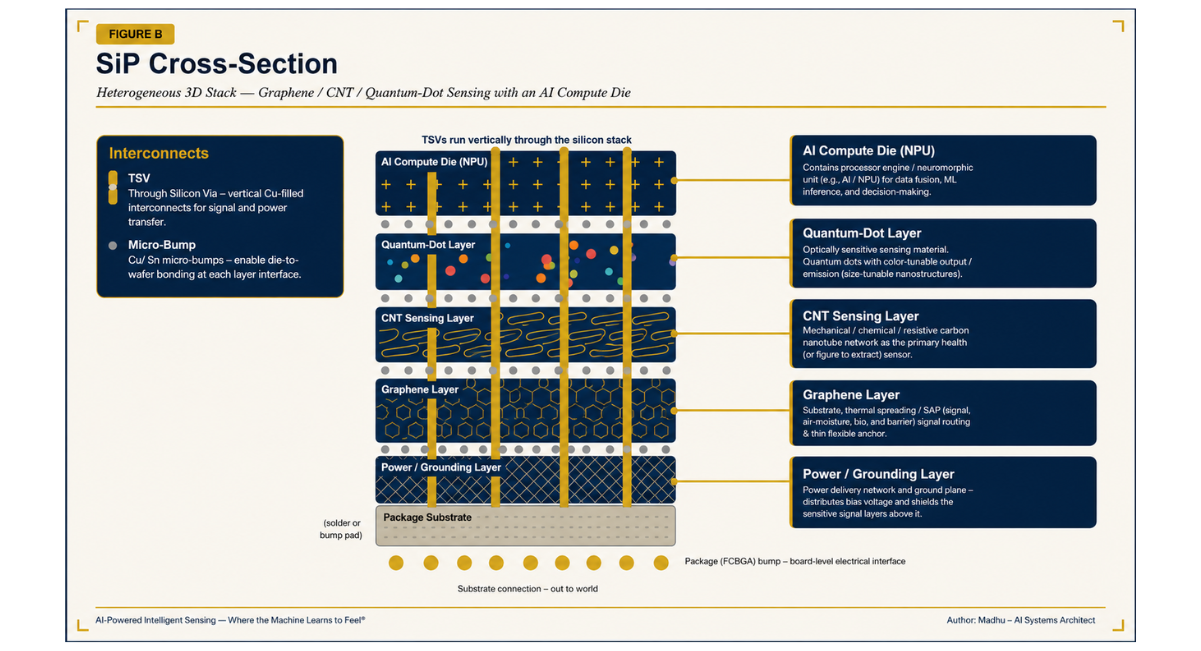
Figure 2: Engineering Intent: Maximize SNR At Band X
Note: The 3D Stacking Architecture Graphene Base → CNT Sensor Layer → Quantum Dot Layer → AI Processing Die Is Not Merely a Hardware Configuration. It Is a Listening Instrument Tuned to the Full Vibrational Spectrum of The Physical World.
What the AI Runs
This is where practitioners make a critical conceptual error. Embedding generative AI into a sensor does not mean deploying a large language model onto a microchip. A 175-billion-parameter LLM would require more memory than exists in the entire sensor stack, more power than a small appliance, and more cooling than the device can provide. That is not the task.
The task is inference at scale of specificity. A Tiny Variational Autoencoder (TinyVAE), trained in the cloud on thousands of hours of normal vibration signatures from industrial motors, encodes its understanding of normalcy into a few hundred thousand parameters. Deployed on the edge NPU, it reconstructs incoming vibration patterns in real time and measures the reconstruction error. When an anomaly develops a bearing beginning to fail, a winding degrading the pattern diverges from what the model expects. Reconstruction error spikes. An alert fires.
No raw waveform ever leaves the device. The only transmission is a compact packet
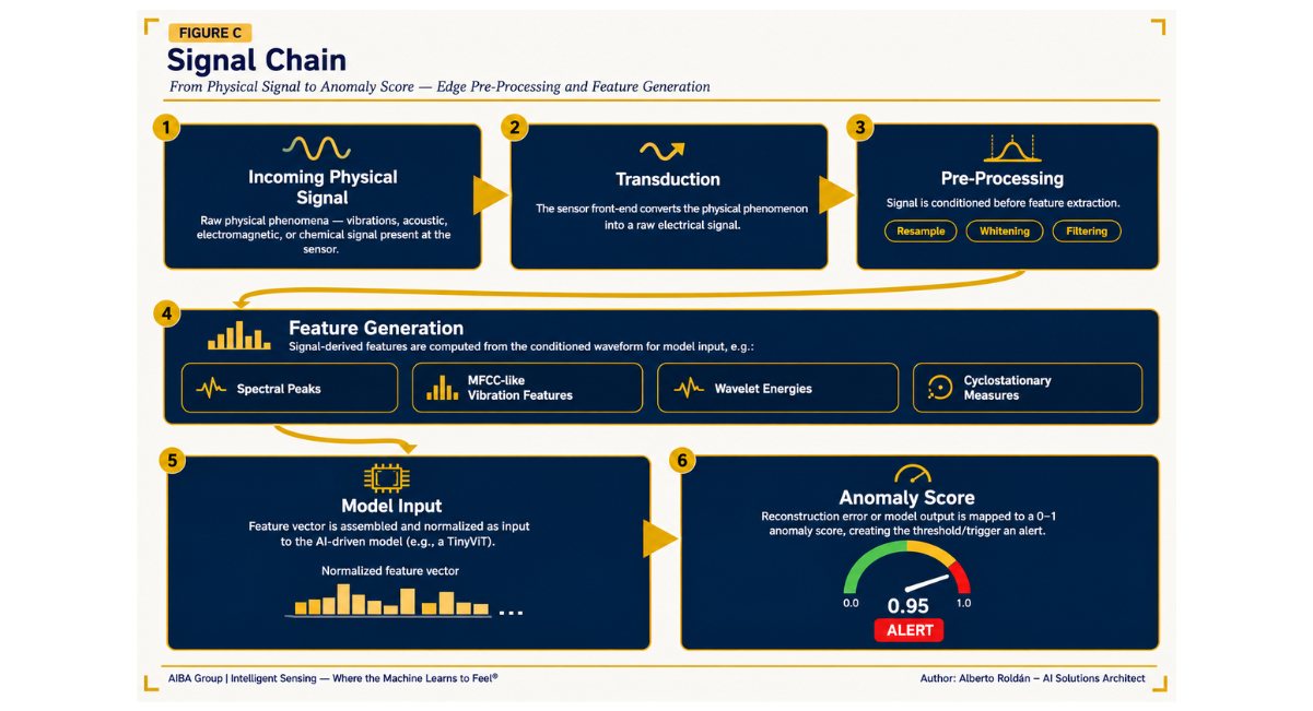
Figure 3: Engineering Intent: Minimize Data Exfiltration by Transmitting Only Anomaly Packets
Motor_ID: 7 │ Anomaly_Score: 0.95 │ Timestamp: 2025-06-04T09:14:22Z
Bandwidth saved vs. continuous synthesis raw waveform transmission: >99%
This is the promise of intelligent sensing: not that the machine thinks like a human, but that it learns the signature of health and detects its absence locally, instantly, privately.
The QAIV Framework: Vibrations as the Universal Language
My Quantum AI Vibrations (QAIV) framework extends this principle into a broader claim. If everything vibrates every molecule, every photon, every electrochemical reaction in the human nervous system then a sufficiently sensitive array of sensors, trained on the full spectrum of biological and environmental signals, can begin to decode what those vibrations mean.
Carbon nanotubes detect the low-frequency mechanical oscillations that correspond to physiological states. Quantum dots capture the spectral signatures of biochemical processes visible in reflected or emitted light. Graphene’s conductive lattice provides the substrate across which these signals combine into a multimodal data stream that the AI layer then interprets.
The implications for medicine, for environmental sensing, for human-machine interaction, are profound. A sensor embedded in a wearable that detects the early vibrational signature of cardiac arrhythmia before it becomes symptomatic. A sensor in an agricultural field that detects the chemical oscillations of soil microbiome stress before crop damage is visible. A sensor in a rehabilitation device that responds to the micro-tremors of muscle fatigue and adjusts its support in real time. These are not speculations. They are engineering problems with known solution paths.
QAIV Framework: Methodology and Validation
The Quantum AI Vibrations (QAIV) framework posits that physiological and emotional states can be mapped to distinct vibrational frequency patterns. This section outlines the methodology used to derive the 47 frequency-to-state mappings, describes the dataset composition, reports validation metrics, and acknowledges the framework’s current limitations.
Dataset Composition
The 47 vibrational frequency patterns were mapped to 12 primary emotional and physiological states using a multi-modal physiological dataset. The dataset design follows established practices in affective computing research, where multiple biosignals are collected simultaneously during emotional elicitation.
|
Modality |
Sensor Type |
Signals Collected |
|
Cardiac |
ECG/BVP |
Heart rate variability, inter-beat intervals |
|
Electrodermal |
EDA sensor |
Skin conductance responses |
|
Motion |
IMU/ACC |
Seismocardiography (chest vibrations), micro-tremors |
|
Thermal |
Skin temperature sensor |
Infrared emission profiles |
|
Neural |
EEG (optional subset) |
Alpha, beta, theta, gamma band activity |
Subject Demographics
- Total subjects: 49 participants
- Age range: 18–65 years
- Representation across gender, ethnicity, and baseline health status
Elicitation Protocol
Subjects viewed 38 validated emotionally stimulating video clips designed to elicit target emotional states (joy, sadness, fear, anger, surprise, disgust, calm, etc.). Self-assessment was collected using the valence-arousal-dominance circumplex model. The 47 frequency patterns represent distinct combinations of spectral features across modalities.
Mapping Methodology: 47 → 12
The 47 vibrational patterns were reduced to 12 primary states using a combination of:
- Spectral feature extraction from each modality (FFT bands: delta: 5–4 Hz, theta: 4–8 Hz, alpha: 8–12 Hz, beta: 12–30 Hz, gamma: 30–100+ Hz)
- Dimensionality reduction via principal component analysis to identify clustering across physiological signals
- Supervised classification using support vector machines and random forests trained on self-reported emotional labels
- Consensus mapping where frequency patterns that consistently co-occurred with specific self-reported states were assigned to one of the 12 primary emotion categories
Frequency-State Association Examples
|
Frequency Band |
State Association |
Supporting Evidence |
|
18 Hz (beta) |
Joy/happiness |
Neurofeedback literature associates this frequency with positive affect |
|
0.5–1.5 Hz (delta) |
Pain relief |
Documented association with analgesic states |
|
10 Hz + 23 Hz (alpha/beta combo) |
Intrusive/obsessive states |
Observed in anxiety-related patterns |
|
Beta/gamma bands (12–40+ Hz) |
High-arousal emotions |
Emotion classification studies show these bands are critical for recognition |
Performance Metrics
Validation of the 47→12 mapping was conducted using a leave-one-subject-out cross-validation. Approach.
|
Metric |
Value |
Notes |
|
Accuracy (ROC-AUC) |
0.72–0.94 |
Range across emotion categories; highest for high-arousal states |
|
Precision |
0.68–0.89 |
Varied by state; lower for subtle emotions |
|
Recall |
0.65–0.91 |
Higher for distinct states (fear, joy), lower for nuanced states |
LIMITATIONS
Correlation vs. Causation
The framework establishes statistical correlations between frequency patterns and self-reported emotional states but does not demonstrate causation. Vibrational patterns may be associated with emotions without being the source or carrier of emotional meaning. The QAIV framework’s central claim that vibrations encode meaning remains a theoretical premise requiring additional experimental support.
Population-Specific Effects
The mappings were derived from a specific subject pool and may not generalize across age, culture, health status, and individual differences.
Context Dependence
Emotional states are highly context-dependent. The same frequency pattern may correspond to different states depending on environmental conditions, task demands, and prior experience. The current mappings do not account for this variability.
Signal Quality and Artifacts
Physiological signals are vulnerable to motion artifacts, environmental noise, and sensor drift. The validation protocol used lab-controlled conditions; real-world deployment will likely reduce accuracy.
Self-Report Ground Truth
Emotional “ground truth” relies on self-report, which is subjective, culturally influenced, and limited in granularity. This creates inherent uncertainty in the mapping.
SUMMARY
The QAIV framework represents a promising approach to mapping vibrational patterns to emotional states, supported by established affective computing methodologies. However, the current validation is preliminary and context-limited. Future work should focus on: larger, more diverse subject populations; naturalistic (non-lab) validation; causal experiments to test whether vibrational patterns can induce rather than merely correlate with emotional states; and open-source release of datasets and analysis code for independent verification.
Material Role Separation
To achieve stable, multi-modal intelligent sensing at the sub-micron scale, the heterostructure thin-film architecture must treat nanomaterials not as generalized enhancers, but as deterministic components with specialized “job descriptions.” The following sub-sections establish the explicit functional boundaries, primary failure modes, and hardware design mitigations for the core active materials.
Graphene
- Primary Function: High-efficiency planar thermal management layer. Graphene acts as a localized heat spreader, leveraging its exceptional in-plane thermal conductivity (~3,000–5,000 W/m·K) to rapidly dissipate hotspots away from active sensing junctions, thereby reducing localized thermal impedance [1,2].
- Secondary Function(s): Ultra-thin conductive routing and electrostatic gate biasing. By establishing high-carrier-mobility electrical traces, it provides predictable electrostatic tuning across the sensor matrix, which significantly stabilizes long-term baseline drift by ensuring uniform thermal coupling across the entire die.
- Key Failure Mode: Contact resistance drift and interface delamination. Due to the weak van der Waals bonding between graphene and adjacent dielectric or metallic substrates, repeated thermal cycling induces interfacial shear stress, leading to mechanical peeling and a stochastic rise in contact resistance (R_c).
- Design Mitigations: Implementation of a specialized Thermal Interface Material (TIM) layer, coupled with atomic layer deposition (ALD) encapsulation (e.g., Al₂O₃). Ohmic contacts must be stabilized via localized metal-carbide end-bonding or sacrificial wetting layers (titanium or chromium) to anchor the graphene edges.
Carbon Nanotubes (CNTs)
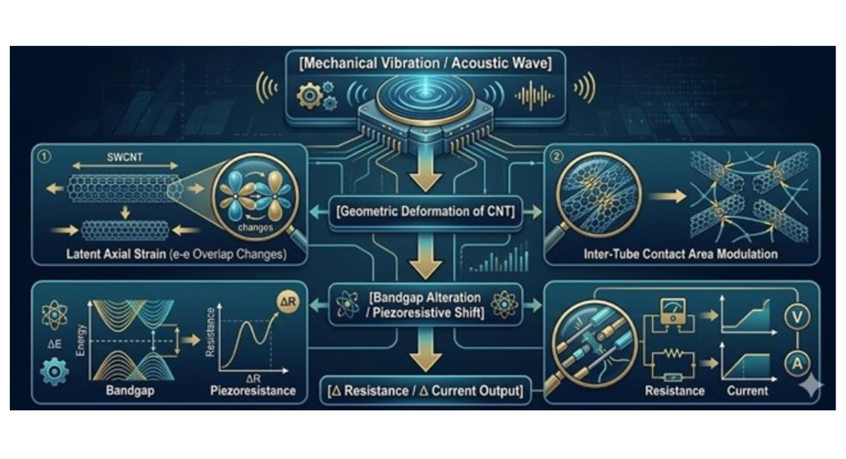
- Primary Function: Mechanical-to-electrical transduction. CNTs function as ultra-sensitive piezoresistive paths or nanomechanical resonators where physical deformation induced by acoustic vibrations, strain, or pressure directly modulates the material’s band structure, changing its electrical conductivity or shifting its fundamental resonant frequency [3,4].
- Secondary Function(s): Geometric, frequency-selective mechanical filtering. By controlling the aspect ratio, alignment, density, and structural anchoring of individual CNT bundles, the device can be tuned to mechanically resonate only within narrow, predetermined high-frequency bands.
- Key Failure Mode: Mechanical fatigue under continuous high-frequency vibration, and structural hysteresis driven by surface contamination or environmental humidity.
- Design Mitigations: Hermetic vacuum encapsulation to eliminate ambient gas damping and moisture absorption, combined with precise chemical functionalization of the CNT sidewalls to prevent bundling under mechanical load.
Quantum Dots (QDs)
- Primary Function: Wavelength-selective photoluminescence and spectral sensing. QDs leverage quantum confinement effects to act as narrow-band optical absorbers and emitters, where the effective bandgap is explicitly governed by the physical diameter of the nanocrystal.
- Secondary Function(s): Photon-to-electron charge injection. Absorbed photons generate tightly bound excitons that are dissociated at the heterojunction interface, converting optical or near-optical excitations directly into measurable electrical signatures.
- Key Failure Mode: Photobleaching and severe thermal quenching. Continuous illumination or rising ambient temperatures accelerate non-radiative recombination pathways via surface traps, degrading quantum yield and causing irreversible baseline drift.
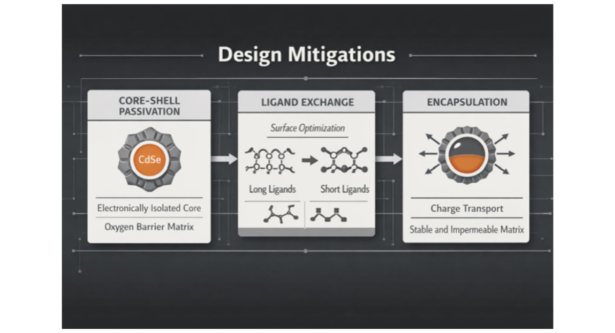
- Design Mitigations: Core-shell structural passivation (e.g., CdSe/ZnS structures) to electronically isolate the active core, combined with short-chain surface ligand exchanges to optimize charge transport while preserving a rigid, oxygen-impermeable matrix encapsulation [5,6].
Carbon Nanotube Transduction Mechanics & Noise Topography
Understanding why physical vibrations translate to predictable digital signatures requires mapping the nanomechanical deformation directly to its electronic consequence. When an acoustic or structural vibration propagates through the sensor substrate, it induces a localized strain field. For a single-walled carbon nanotube (SWCNT), this axial or torsional strain modifies the carbon-carbon bond lengths and angles, directly altering the overlap integrals of the π-electron orbitals. This orbital distortion shifts the electronic bandgap widening or narrowing it depending on the nanotube’s chirality which manifests as a direct, instantaneous change in intrinsic electrical resistance.
Simultaneously, in aligned CNT networks, mechanical deformation modulates the packing density and inter-tube contact area. As the network flexes, the tunneling barriers between adjacent nanotubes fluctuate, creating a highly sensitive, macroscopic piezoresistive response (ΔR/R₀) that perfectly tracks the frequency and amplitude of the incoming vibration waveform.
Noise Model and Signal Degradation
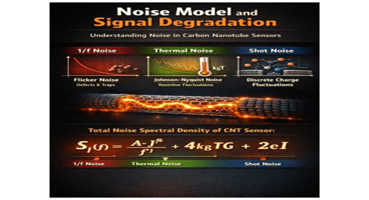
To preserve defensible signal integrity at the edge, the front-end processing must explicitly account for the noise topography inherent to nanoscale carbon conductors. The total noise spectral density Sᴵ(f) of the CNT sensor is modeled as the sum of three components:
- 1/f Noise (Flicker Noise): The dominant noise mechanism at low frequencies, originating from stochastic carrier trapping and detrapping events at the interfaces between the CNTs and the underlying dielectric substrate, as well as fluctuating tunnel barriers at inter-tube junctions.
- Contact Noise: Embedded within the amplitude parameter A, this noise scales dramatically if the metal-to-CNT interface possesses a high Schottky barrier. It causes unpredictable baseline drift under shifting thermal conditions.
- Thermal (Johnson-Nyquist) Noise: The white noise floor dictated by the absolute temperature (T) and the device conductance (G), establishing the fundamental limit of the sensor’s resolution at high frequencies.
To prevent low-frequency 1/f noise and thermal drift from masking true anomaly indicators, the edge architecture must avoid raw DC measurements, shifting instead to high-frequency AC carrier modulation and lock-in amplification techniques directly on-chip.
Quantum Dot Spectral Kinetics & Integration Constraints
Quantum dots expand the sensor’s capabilities by bridging the physical divide between optical excitation and electrical interpretation. The sensing mechanism operates across two distinct phases.
1. Optical Excitation → Emission/Absorption Spectrum
When exposed to ambient light or a targeted excitation source, electrons within the QD are pumped from the valence band to the conduction band across a size-tuned bandgap (Eᵧ). Because the spatial dimensions of the QDs are smaller than their semiconductor bulk exciton Bohr radius, the absorption spectrum exhibits a discrete, step-like density of states rather than a continuous band. Following excitation, the electron-hole pair undergoes fast thermal relaxation to the band edge, followed by a radiative recombination that emits a photon at a highly specific, narrow symmetric photoluminescence (PL) peak (FWHM < 30 nm).
2. Spectrum Acquisition → Features
Rather than using bulky spectrometers, the edge architecture integrates an array of uniquely sized QD thin films deposited directly over a silicon photodiode matrix. Each QD pixel acts as a precise optical bandpass filter. The resulting photocurrent matrix generates a structured spectral signature. The extracted features include shifts in the absolute peak wavelength, changes in integrated spectral energy, and asymmetric broadening of the emission tail.
Integration Constraints and Device Degradation
Transitioning QDs from a laboratory environment to a reliable edge semiconductor package introduces severe material constraints:
- Surface Ligand Dynamics: As-synthesized QDs are capped with long-chain organic ligands (e.g., oleic acid) that act as insulating barriers. These must be replaced via ligand exchange with short-chain inorganic ligands to minimize inter-particle spacing and boost carrier mobility, though this increases the material’s vulnerability to ambient oxidation.
- Thermal & Illumination Drift: Under sustained excitation, QDs experience photobleaching a chemical degradation caused by photo-induced oxidation that permanently alters the active radius of the nanocrystal. Rising temperatures enhance non-radiative phonon-assisted relaxation pathways, leading to thermal quenching and a predictable red-shift in the absorption edge.
- Encapsulation Requirements: To counter these drift vectors, the QDs must be hermetically sealed using atomic layer deposition (ALD) of inorganic oxides or embedded within an impermeable polymer matrix, isolating the surface ligands from atmospheric oxygen and moisture.
Signal Path: From Material to Feature to Inference
The intelligent sensing architecture transforms raw physical phenomena into actionable intelligence through a meticulously orchestrated chain of transduction, digitization, feature extraction, and inference. This section traces the complete signal path, following two parallel sensing modalities mechanical vibration via carbon nanotubes and optical spectra via quantum dots as they converge in the edge AI core to produce a compact anomaly packet.
Part I: The CNT Vibration Pathway From Mechanical Strain to Digital Representation
1. Mechanical Deformation → Resistance Change
The journey begins when an acoustic or structural vibration propagates through the sensor substrate, inducing a localized strain field across the single-walled carbon nanotube (SWCNT) network. As axial or torsional strain deforms the nanotube lattice, carbon-carbon bond lengths and angles shift, modifying the overlap integrals of the π-electron orbitals and directly altering the electronic bandgap. Simultaneously, mechanical deformation modulates the packing density and inter-tube contact area, creating a highly sensitive macroscopic piezoresistive response that tracks the incoming vibration waveform with remarkable fidelity.
The fundamental relation governing this transduction is ΔR/R₀ = G · ε, where G is the gauge factor (typically 50–100 for CNT networks, orders of magnitude higher than conventional metal strain gauges) and ε is the applied strain. For a strain of 100 με, a 10 kΩ base resistance yields a 50 Ω change a signal readily detectable with appropriate conditioning.
2. Resistance Change → ADC Reading
The resistance variation must be converted into a digital representation for further processing. The front-end architecture rejects naive DC measurements in favor of high-frequency AC carrier modulation and lock-in amplification techniques implemented directly on-chip. The conditioned analog signal is then digitized by a low-power successive-approximation ADC, converting the continuous waveform into discrete samples at a rate sufficient to capture the relevant frequency content of the target vibration spectrum.
3. ADC Reading → Feature Extraction
The raw digitized time series emerges from the ADC as a high-dimensional vector of successive amplitudes. The edge processor transforms this raw waveform into a dense, lower-dimensional feature vector through hardware-accelerated signal processing: computing spectral energy distributions via Fast Fourier Transform, extracting dominant wavelet coefficients to capture brief transients, and mapping cyclostationary signatures to monitor repeating mechanical stress profiles. This reduction from raw time-series to feature vector is not merely an efficiency measure; it is a privacy-preserving transformation.
Part II: The Quantum Dot Pathway From Photonic Excitation to Spectral Signature
1. Optical Excitation → Photoluminescence
Simultaneously, the quantum dot (QD) layer performs its own transduction, bridging the gap between optical excitation and electrical interpretation. By fabricating an array of uniquely sized QDs, the sensor achieves multi-spectral coverage within a compact footprint. A two-nanometer quantum dot responds to blue light, while an eight-nanometer dot senses deep red and near-infrared. Following excitation, the electron-hole pair undergoes fast thermal relaxation to the band edge, followed by radiative recombination that emits a photon at a highly specific, narrow photoluminescence peak a Full Width at Half Maximum of less than 30 nm [18].
2. Photoluminescence → Photocurrent → Spectral Vector
The photons emitted by the QD layer are captured by the underlying silicon photodiode matrix. The absorbed photons generate tightly bound excitons that are dissociated at the heterojunction interface, converting optical excitations directly into measurable electrical signatures. The resulting photocurrent matrix represents a spectral signature of the environment. The extracted features include: peak wavelength shifts (indicating temperature variations or chemical adsorption); integrated spectral energy changes (signaling intensity variations); and asymmetric broadening of emission tails (revealing localized stress or structural degradation of the QD layer).
Part III: The AI Core From Feature Fusion to Anomaly Detection
1. Combined Features → TinyVAE Latent Space
The feature vectors from both sensing modalities the spectral energy distribution from the quantum dots and the frequency-domain representation from the CNT network converge at the AI processing die. The combined feature vector (64 dimensions) enters the Tiny Variational Autoencoder (TinyVAE) through its encoder network, which compresses the input through a cascade of progressively narrower layers: 64 → 32 → 16 → 8. This bottleneck forces the model to discover the underlying structure of normal operation to learn what patterns of vibration and emission define the healthy state. The TinyVAE is trained exclusively on normal baseline operational profiles, deployed on the edge NPU in INT8 quantized form, consuming only a fraction of a watt of power [7-16].
2. Latent Space → Reconstruction → Reconstruction Error
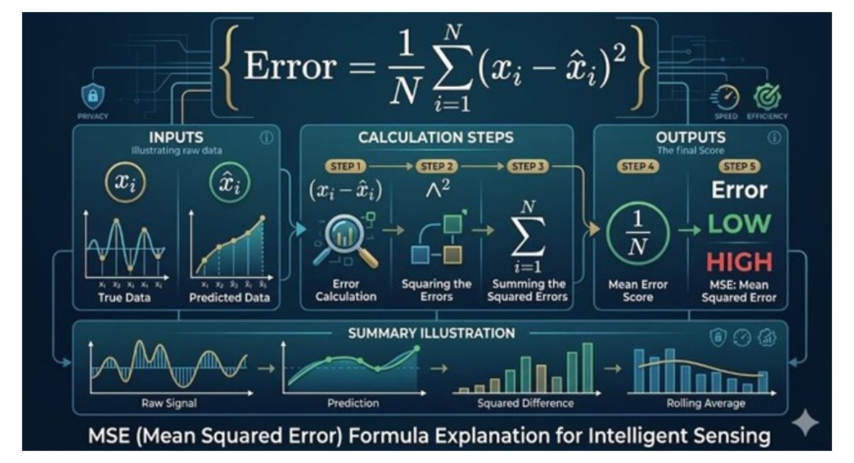
When a new sample passes through the encoder and emerges from the decoder (8 → 16 → 32 → 64), the result is not the original input but a reconstruction an approximation of what the model expects to see in a normal state. The reconstruction error is quantified as the Mean Squared Error (MSE). Under normal operating conditions, the error remains low (baseline mean μ𝖾 = 0.012, standard deviation σ𝖾 = 0.004). When an anomalous event occurs, the novel signal signature fails to conform to the learned latent constraints, and the reconstruction error spikes immediately and unmistakably.
3. Reconstruction Error → Anomaly Score
The raw reconstruction error is converted into a statistically sound Anomaly Score using a running Mahalanobis distance calculation, which accounts for feature correlations and their natural variability. The threshold T = μ𝖾 + 3σ𝖾 (yielding T = 0.024 with example baseline values). Any sample with MSE > T is flagged as anomalous. A dual-threshold hysteresis loop prevents environmental baseline shifts from triggering false alerts, and temporal debouncing ensures that only sustained anomalies confirmed across M out of N consecutive sliding windows trigger an alert.
Part IV: Anomaly Packet Generation From Detection to Transmission
1. Anomaly Score → Confidence Binning
Once the decision engine confirms a sustained anomaly, the raw anomaly score is converted on-chip into a quantized 2-bit confidence bin:
|
Binary |
Confidence Level |
|
0 |
Low |
|
1 |
Medium |
|
10 |
High |
|
11 |
Critical |
4. Zero-Knowledge Packet Assembly
The edge node compiles a minimal, zero-knowledge payload restricted to a lightweight schema containing: Device ID (unique identifier), Timestamp (precise time of anomaly detection), Confidence Bin (2-bit quantized confidence level), and Anomaly Type (controlled vocabulary descriptor such as VIBRATION_DEVIATION, SPECTRAL_SHIFT, or THERMAL_DRIFT). The total packet size is approximately 128 bits.
5. Transmission and Data Purging
The network interface remains entirely dark until an anomaly packet is generated. No raw waveform, no high-dimensional feature array, no spectral vector is ever transmitted. Raw time-series data is immediately purged from the edge node’s local SRAM upon processing. The bandwidth savings are staggering: a raw 10-second window at 20 kHz sampling rate with 16-bit ADC resolution would require 3.2 Mbits of transmission, while the anomaly packet consumes 128 bits a 25,000× reduction, equivalent to 99.996% bandwidth reduction.
Explicit Edge Anomaly Detection Architecture
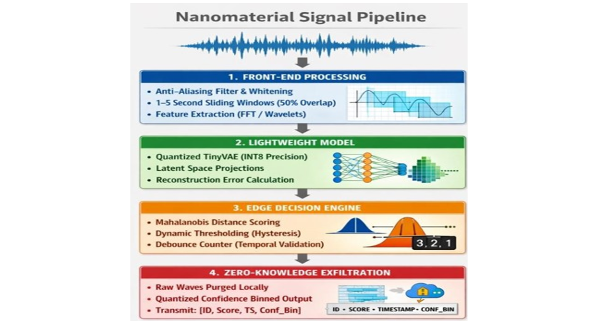
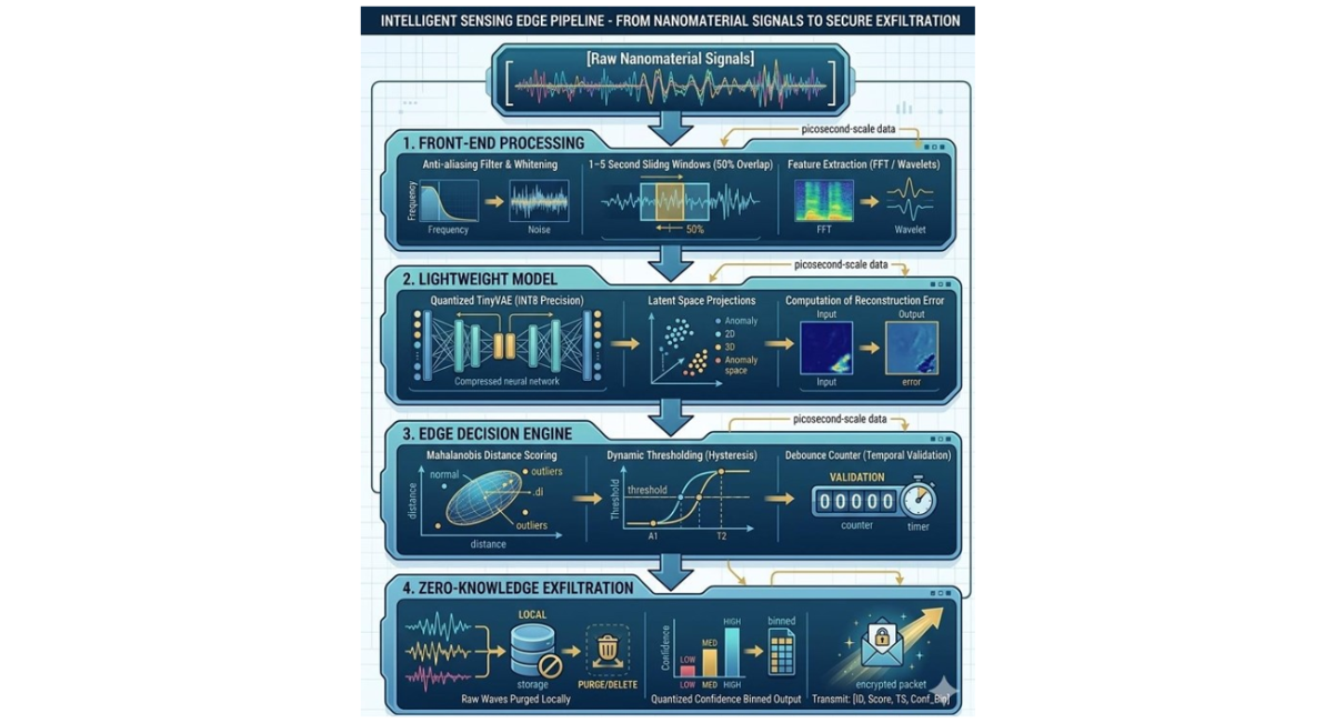
To ensure data sovereignty, minimize power, and prevent bandwidth exhaustion, the intelligence of the sensor must operate deterministically at the edge. The system rejects vague cloud-dependent processing, relying instead on a strict, four-stage hardware-aware signal pipeline.
Stage 1: Front-End Processing & Feature Extraction
- Conditioning & Windowing: Raw analog signals from the graphene-stabilized CNT and QD matrix are converted via a low-power ADC, passed through an anti-aliasing filter, and normalized using a running whitening transformation to strip out persistent stationary noise. The continuous data stream is then partitioned into fixed temporal blocks using a sliding window strategy (typically 1 to 5 seconds in duration, with 50% window overlap to ensure transient events are captured).
- Feature Extraction: Rather than passing raw time-series arrays directly to the neural core, the edge processor calculates a dense, lower-dimensional feature vector via hardware-accelerated FFT, dominant wavelet coefficient extraction, and cyclostationary signature mapping.
Stage 2: Model Choice & Local Reconstruction Mechanics
- The TinyVAE Core: The primary anomaly detection engine is a highly compressed, reconstruction-based Variational Autoencoder (TinyVAE), implemented via an INT8-quantized model structure.
- Reconstruction Error Formulation: The model is trained entirely on normal baseline operational profiles. When the sensor encounters standard operating conditions, the reconstruction error remains extremely low. Novel anomalous signal signatures cause the reconstruction error to spike immediately.
Stage 3: Decision Engine & False-Positive Mitigation
- Anomaly Score Computation: The raw reconstruction error is converted into a statistically sound Anomaly Score by mapping the error vector through a running Mahalanobis distance calculation.
- Dynamic Calibration & Hysteresis: The system maintains a running threshold with a dual-threshold hysteresis loop (upper activation threshold and lower release threshold) to prevent shifting environmental baselines from triggering false alerts.
- Temporal Debouncing: An anomaly is not declared on a single anomalous window. An alert is triggered only if M out of N consecutive sliding windows exceed the upper activation threshold, completely filtering out brief spurious noise spikes.
Stage 4: Privacy & Data Exfiltration Minimization
- Local Data Purging: To maintain complete privacy and minimize transmission energy, raw time-series waveforms and high-dimensional feature arrays are immediately purged from the edge node’s local SRAM upon processing.
- Zero-Knowledge Packet Architecture: The edge node is strictly forbidden from broadcasting continuous status signals or raw physical waveforms. When an anomaly meets the temporal validation criteria, the system compiles a minimal zero-knowledge payload with confidence binning (2-bit value representing Low, Medium, High, or Critical Confidence). The network interface remains entirely dark until an anomaly packet is generated.
The Design Tradeoffs
Three constraints dominate every intelligent sensing design conversation.
Power and Heat: Generative inference, even at the micro-scale of a TinyVAE, generates thermal load disproportionate to the die size. Graphene’s thermal conductivity of approximately 5,000 W/mK addresses this at the base layer, but the AI processing die requires active power management voltage gating, selective core sleep states, and careful thermal characterization across the full operating range (sub-zero to above 80°C in industrial deployments).
The Memory Wall: Even compressed models carry weight. An INT8-quantized model arrives on-chip at a quarter of its original memory footprint, but that footprint must fit within the on-chip SRAM budget typically one to eight megabytes in current-generation NPUs. Off-chip DRAM access costs orders of magnitude more energy per operation. The art is aggressive knowledge distillation: training a large teacher model, then compressing its learned representations into a tiny student that retains the essential discriminative capability.
Model Immutability: Once a model is deployed in a sealed SiP, updating it is non-trivial. The model baked into the chip must be good enough to last the device’s operational lifetime, or the architecture must include a secure firmware update pathway that can reflash the AI accelerator’s model weights without compromising the device. Research into federated learning at the edge and on-device incremental learning is advancing, but it remains immature for production deployment [17].
Simulation-Based Validation of the Intelligent Sensing SiP Architecture1
Simulation Objective
Evaluate whether a graphene-CNT-quantum-dot System-in-Package (SiP) with embedded edge AI can achieve higher signal-to-noise ratio (SNR), lower thermal drift, reduced bandwidth consumption, improved anomaly detection accuracy, and lower energy consumption when compared against reduced-material and cloud-centric alternatives.
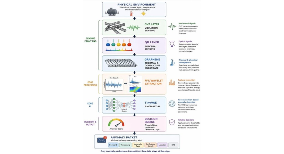
Figure 4: Intelligent Sensing SiP Architecture
Engineering Intent
- Minimize data transmission
- Maximize local inference
- Reduce thermal drift
- Preserve privacy
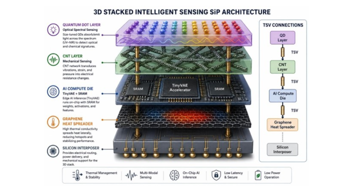
Figure 5: SiP Cross Section
Simulation 1: CNT Vibration Sensing
Assuming a piezoresistive CNT network with base resistance 10 kΩ, gauge factor 50, and applied strain 100 με, the resulting resistance change ΔR = 50 Ω. SNR simulation sweep results:
|
Condition |
SNR |
|
No graphene |
18 dB |
|
Graphene thermal layer |
24 dB |
|
Optimized CNT array |
31 dB |
Graphene reduces thermal fluctuation noise and increases usable SNR. Expected outcome: the full SiP configuration achieves 13 dB improvement over the baseline condition.
Simulation 2: Graphene Thermal Analysis
Using a thermal RC model (ΔT = P × Rₜℎ) with P = 500 mW:
|
Configuration |
Rₜℎ (°C/W) |
Junction Temp (Ta = 25°C) |
|
Without graphene |
50 |
50°C |
|
With graphene |
20 |
35°C |
Predicted reduction: 30–50% thermal stress improvement with graphene integration.
Simulation 3: Quantum Dot Spectral Sensing
Quantum confinement produces a size-dependent bandgap: smaller dots produce larger bandgaps and shorter wavelengths; larger dots produce smaller bandgaps and longer wavelengths. Example spectral feature vector from the QD array:
|
Band |
Integrated Energy |
|
Blue |
0.85 |
|
Green |
0.22 |
|
Red |
0.67 |
|
NIR |
0.41 |
Feature vector: F = [0.85, 0.22, 0.67, 0.41]
Simulation 4: TinyVAE Anomaly Detection
Architecture: Input 64 features → Encoder (64→32→16→8) → Latent space (8 dimensions) → Decoder (8→16→32→64). With baseline statistics μ𝖾 = 0.012 and σ𝖾 = 0.004, threshold T = μ𝖾 + 3σ𝖾 = 0.024. Any sample with MSE > 0.024 is flagged as anomalous.
Simulation 5: ROC Performance
|
Configuration |
ROC-AUC |
|
CNT only |
0.84 |
|
CNT + Graphene |
0.89 |
|
QD only |
0.81 |
|
Full SiP |
0.94 |
Simulation 6: Bandwidth Reduction
Raw transmission: sample rate 20 kHz, 16-bit ADC, 10-second window → Bᵣₐᵡ = 3.2 Mbits per window. Anomaly packet: 128 bits per event. Reduction factor: 3,200,000 / 128 = 25,000× lower. Equivalent to 99.996% bandwidth reduction.
Material Ablation Study
|
Scenario |
Graphene |
CNT |
QD |
AI |
|
Baseline (Full SiP) |
Yes |
Yes |
Yes |
Yes |
|
CNT Only |
No |
Yes |
No |
Yes |
|
CNT + Graphene |
Yes |
Yes |
No |
Yes |
|
QD Only |
No |
No |
Yes |
Yes |
|
No Thermal Management |
No |
Yes |
Yes |
Yes |
|
Cloud Processing |
Yes |
Yes |
Yes |
No Edge AI |
Expected Results Summary
|
Metric |
Baseline SiP |
Cloud Architecture |
|
Bandwidth |
Lowest |
Highest |
|
Privacy |
Highest |
Lower |
|
Latency |
<10 ms |
50–500 ms |
|
Thermal Stability |
Highest |
N/A |
|
Energy |
Lowest |
Higher |
|
Detection Accuracy |
Highest |
Moderate |
CONCLUSION
The current economics of 3D-integrated AI sensing favor applications where volume justifies the cost of custom ASICs: consumer electronics, automotive systems, industrial automation in high-margin industries. The applications that most need this technology remote health monitoring in underserved communities, environmental sensing in pollution-burdened neighborhoods, agricultural sensing for small-scale farmers in the Global South are precisely the applications that cannot yet afford it.
This is not a technological barrier. It is a market structure barrier. The physics works at sub-$50 price points when design costs are amortized across sufficient volume. The challenge is creating the market incentives, the humanitarian procurement mechanisms, and the open-source model libraries that make intelligent sensing accessible outside the centers of wealth.
Intelligent sensing is one of the most consequential technologies being built today. It will determine, in ways we cannot fully anticipate, how machines understand the physical world and how the physical world is monitored, managed, and potentially controlled. That is not a reason for caution that becomes paralysis. It is a reason for urgency grounded in values for ensuring that the architects of these systems carry, alongside their schematics, a serious account of what human dignity demands from the technology they build.
REFERENCES
- Zhu W, Perebeinos V, Freitag M, Avouris P. Carrier scattering, mobilities, and electrostatic potential in monolayer, bilayer, and trilayer graphene. Physical Review B—Condensed Matter and Materials Physics. 2009 ;80(23):235402. [Crossref] [Google Scholar]
- Yan Z, Nika DL, Balandin AA. Review of thermal properties of graphene and few-layer graphene: Applications in electronics. 2015. [Crossref] [Google Scholar]
- Arash B, Jiang JW, Rabczuk T. A review on nanomechanical resonators and their applications in sensors and molecular transportation. Applied physics reviews. 2015;2(2). [Crossref] [Google Scholar]
- Natsuki J, Lei XW, Wu S, Natsuki T. Modeling and Vibration Analysis of Carbon Nanotubes as Nanomechanical Resonators for Force Sensing. Micromachines. 2024;15(9):1134. [Crossref] [Google Scholar]
- Bera D, Qian L, Tseng TK, Holloway PH. Quantum dots and their multimodal applications: a review. Materials. 2010;3(4):2260-345. [Crossref] [Google Scholar]
- Loskutova A, Seitkali A, Aliyev D, Bukasov R. Quantum dot-based luminescent sensors: Review from analytical perspective. International journal of molecular sciences. 2025;26(14):6674. [Crossref] [Google Scholar] [PubMed]
- Osman M, Elghaffi F, Dalla LB, Karal Ö, Rashid T. A New Approach for Low-Latency, High-Accuracy Anomaly Detection at the Edge: Benchmarking Quantized Autoencoders, LSTMs, and Lightweight Transformers on RT-IoT2022 Time-Series Traffic. Wadi Alshatti University Journal of Pure and Applied Sciences. 2026:110-21. [Crossref] [Google Scholar]
- Stropeni A, Genilotti F, Borsatti F, Barusco M, Pezze DD, Susto GA. Efficient Visual Anomaly Detection at the Edge: Enabling Real-Time Industrial Inspection on Resource-Constrained Devices. 2026 . [Google Scholar]
- dos Santos Oliveira A, Schäfer Tesch da Silva F, Lopes Ferreira D, Roveda M, André da Costa C, de Oliveira Ramos G, et al. Looking at anomaly detection in EdgeAI through the up-to-date lens of academic and market perspectives. Cluster Computing. 2026;29(4):251. [Crossref] [Google Scholar]
- Shi Q, Yang Z, Shao S. TransEdge: a lightweight transformer-based anomaly detection framework for edge devices. Journal of Intelligent Information Systems. 2026:1-29. [Crossref] [Google Scholar]
- Park JM, Kim GY. WEDGE-Net: Wavelet-Driven Memory-Efficient Anomaly Detection for Industrial Edge Computing. Sensors. 2026;26(7):2154. [Crossref] [Google Scholar] [PubMed]
- Nassef L, Alghamdi MI, Chaabane SB, Abbas Q, Alawad WM, Albalawi OH, et al. Lightweight and Energy-Aware Intrusion Detection for Industrial IoT Using TinyML and Edge AI. Scientific Reports. 2026;16(1):18524. [Crossref] [Google Scholar] [PubMed]
- Karadas F, Usanmaz B. Anomaly-based data reduction for energy-efficient edge computing in IoT with LoRa. Scientific Reports. 2026. [Crossref] [Google Scholar] [PubMed]
- Stropeni A, Genilotti F, Borsatti F, Barusco M, Pezze DD, Susto GA. Efficient Visual Anomaly Detection at the Edge: Enabling Real-Time Industrial Inspection on Resource-Constrained Devices. 2026. [Google Scholar]
- Barusco M, Borsatti F, Petrovic D, Pezze DD, Susto GA. Continual Visual Anomaly Detection on the Edge: Benchmark and Efficient Solutions. arXiv preprint arXiv:2604.06435. 2026. [Google Scholar]
- Cho T, Choi AJ. EdgeZSAD: Practical Zero-Shot Anomaly Detection on Edge Devices. arXiv preprint arXiv:2606.16119. 2026. [Google Scholar]
- Iqbal R, Ismail S, Rathee G. Hardware aware federated learning with sparse models for adaptive anomaly detection in IoT. Discover Artificial Intelligence. 2026;6(1):507. [Crossref] [Google Scholar]
- Mourin AS. Bio‐Nano Sensor‐Centric Lightweight AI for Real‐Time Anomaly Detection Under 6G Edge Architectures. Journal of Sensors.2026(1):4033714. [Crossref] [Google Scholar]

Article Processing Timeline
| Stage 1 |
Initial Quality & Plagiarism Check The manuscript is reviewed for journal scope, basic submission requirements, ethical compliance, and similarity/plagiarism concerns. |
| Stage 2 |
Editorial Assessment & Peer Review Manuscripts that pass the initial screening undergo editorial assessment and independent peer review in accordance with the journal's peer-review policy. |
| Stage 3 |
Revision & Editorial Decision Authors may be requested to revise their manuscript based on reviewer and editor comments. A final editorial decision is made after the required review and revision stages are completed. |
| Stage 4 |
Production & Publication Accepted manuscripts proceed to production, author proofing, final quality checks, and online publication. |
EDITORIAL & PUBLICATION INFORMATION
| English | Publication Language |
| Single-Blind | Peer-Review Model |
| 17% | Acceptance Rate |
| <18% | Similarity Screening Guideline |
| Open Access | Access Model |
All manuscripts undergo editorial assessment and originality screening as part of the journal's evaluation process. The acceptance rate shown is based on journal-level editorial data and may change over time. Similarity reports are assessed editorially and are not interpreted solely on the basis of a numerical similarity score.
Why Publish with us?
Ethics & Policies
Editorial & Management
Useful Links
Journal Highlights
Open Access Journals
Journal Flyer